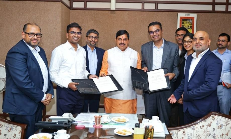
Paras Defence and Space Products, the defence arm of the Paras Group, has signed a memorandum of understanding to establish a ₹6,200 crore semiconductor packaging facility in Madhya Pradesh, marking a significant step in India’s push to build indigenous semiconductor manufacturing capacity for defence applications.
The facility will focus on semiconductor packaging and testing, critical stages in the semiconductor supply chain where raw silicon dies are encased in protective packages and validated for performance. This manufacturing capability addresses a longstanding vulnerability in India’s defence industrial base, where dependence on imported semiconductor components has constrained the pace of domestic weapon system production and modernisation.
India’s defence and space sectors consume specialised semiconductors for radar systems, guidance packages, communication equipment, electronic warfare suites, and sensor integration across platforms ranging from combat aircraft and naval vessels to missile systems and unmanned platforms. Indigenous packaging capacity reduces lead times, enhances supply security, and aligns with the government’s Make in India and Atmanirbhar Bharat objectives in defence manufacturing.
The semiconductor industry in India has historically relied on foundries and packaging units concentrated outside the country, with geopolitical and trade tensions creating logistical bottlenecks. DRDO and the Ministry of Defence have prioritised semiconductor self-sufficiency as a national defence imperative, particularly following global supply chain disruptions during the pandemic and ongoing semiconductor shortages affecting defence procurement timelines.
Paras Defence, a recognised defence contractor with expertise in aerospace components and systems, brings manufacturing discipline and quality control protocols essential for defence-grade semiconductor operations. The Madhya Pradesh location provides access to industrial infrastructure, skilled labour, and proximity to DRDO facilities and defence PSU plants that would be among the primary users of the packaged semiconductors.
The packaging stage, though less capital-intensive than fabrication, demands precision engineering, clean room environments, and rigorous testing protocols to ensure components meet military specifications for temperature extremes, vibration resistance, and electromagnetic hardening. This facility would support both current defence platform production and the next generation of systems under development across the Indian armed forces.
India’s semiconductor ambitions extend beyond packaging; the government has announced plans for a national semiconductor mission to develop fabrication capacity. However, packaging units represent an achievable intermediate milestone that can be operationalised faster and serve as anchors for a broader semiconductor ecosystem centred on defence requirements.
-

-

-

-